
The future of microelectronics starts at ASU
Powering tomorrow’s technology starts with you. Discover how you can be part of what’s next!
The U.S. semiconductor industry is growing fast — are you ready to grow with it?
Experts project a 33% increase in microelectronics jobs by 2030, growing from approximately 345,000 today to over 460,000. That means more opportunities for engineers, technicians, innovators and problem-solvers like you.
At the Ira A. Fulton Schools of Engineering at Arizona State University, we are preparing the next generation of microelectronics professionals. Here’s how you can get started:

Start building job-ready semiconductor technician skills
Looking for a hands-on pathway into Arizona’s semiconductor workforce? ASU’s Foundations for Equipment Technician Program offers no-cost, in-person training aligned to the practical skills used by equipment technicians in advanced manufacturing environments.
We have opportunities for everyone

College students
Learn how can you can make the most of your education and get prepared for a career in microelectronics.
We have lots of options for prospective, current and returning students, including
- Degree programs.
- Hands-on research.
- Internships with top companies.
- Access to advanced facilities

Professionals
How can you reapply your professional experience to expand your career into microelectronics?
Upskill or reskill in the Fulton Schools at ASU. Our pathways combine flexibility, industry relevance and stackable credentials to help you achieve the next level:
- More than six microelectronics fields to choose from
- Flexible, stackable microcredentials that lead to certificates
- Short courses for quick upskilling

K–12 outreach
Students, families, educators and school leaders across Arizona can find their entry point into microelectronics with the Fulton Schools and ASU.
Students and families: Browse hands-on STEM opportunities for all ages, both online and in person.
Educators and administrators: Discover classroom resources and immersive STEM experiences, as well as partnership pathways for schools, all designed to build the state’s semiconductor workforce.
Be part of Arizona’s microelectronics future
The future of technology is being built right here in Arizona. With a booming semiconductor industry, the CHIPS Act fueling innovation and ASU at the forefront of advanced packaging and microelectronics education, this is a once-in-a-generation opportunity to get involved.
ASU leads the development of the next wave of microelectronics talent. Watch this video to learn how advanced packaging is shaping the future — and how you can be part of it through the many microelectronics educational opportunities in the Fulton Schools.
Fulton Schools microelectronics news
-
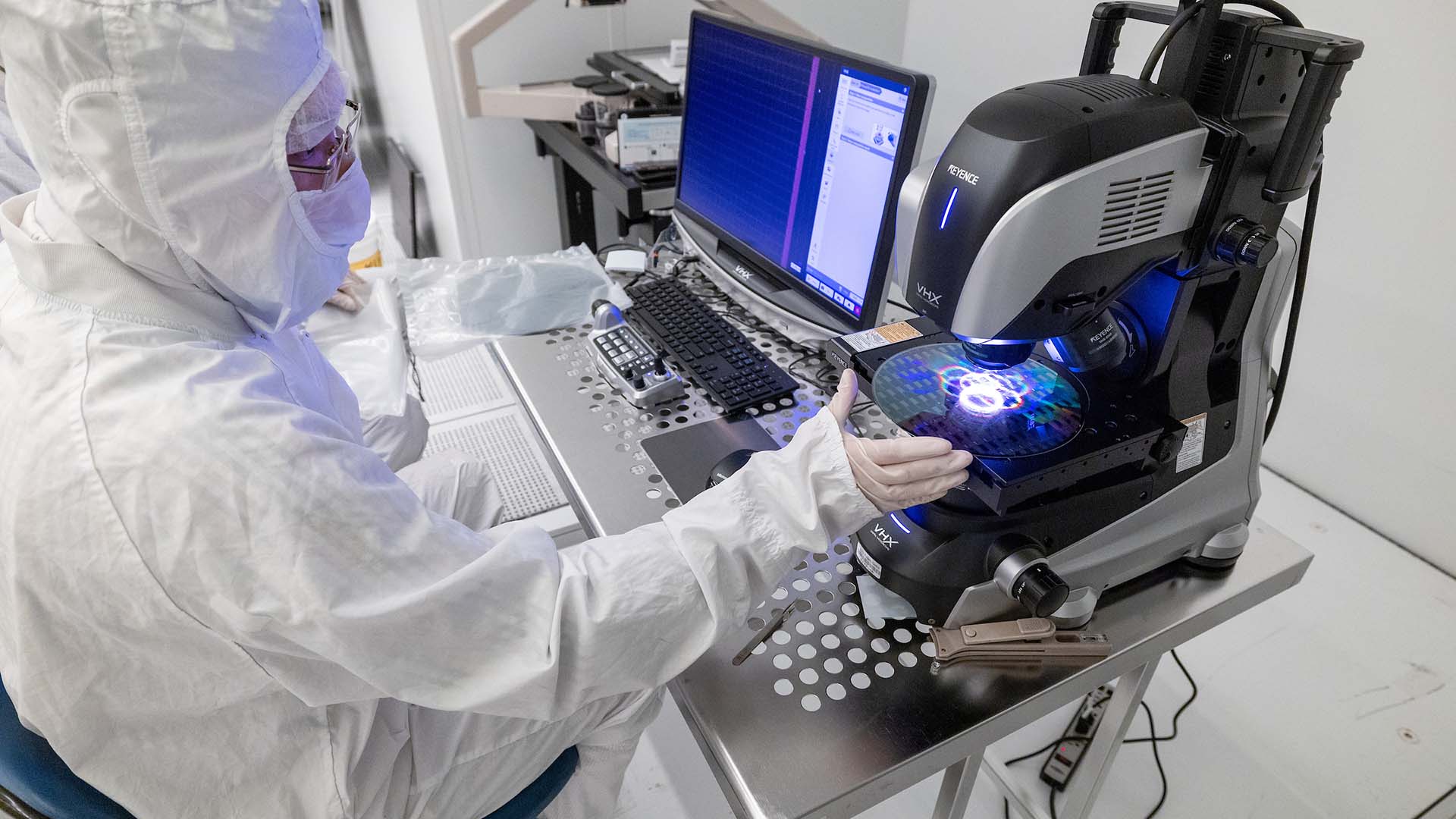
Semiconductor Packaging REU
Explore semiconductor packaging at ASU’s cutting-edge labs. Earn $4,000, get housing, and work with industry leaders like Intel.
-

ASU researcher honored with Google award for AI-driven chip design
Vidya Chhabria receives funding and mentorship to push the boundaries of electronic design automation
-

Tiny chips, big innovations
ASU and Applied Materials charge into the atomic frontier of semiconductor breakthroughs.