Semiconductor Packaging REU
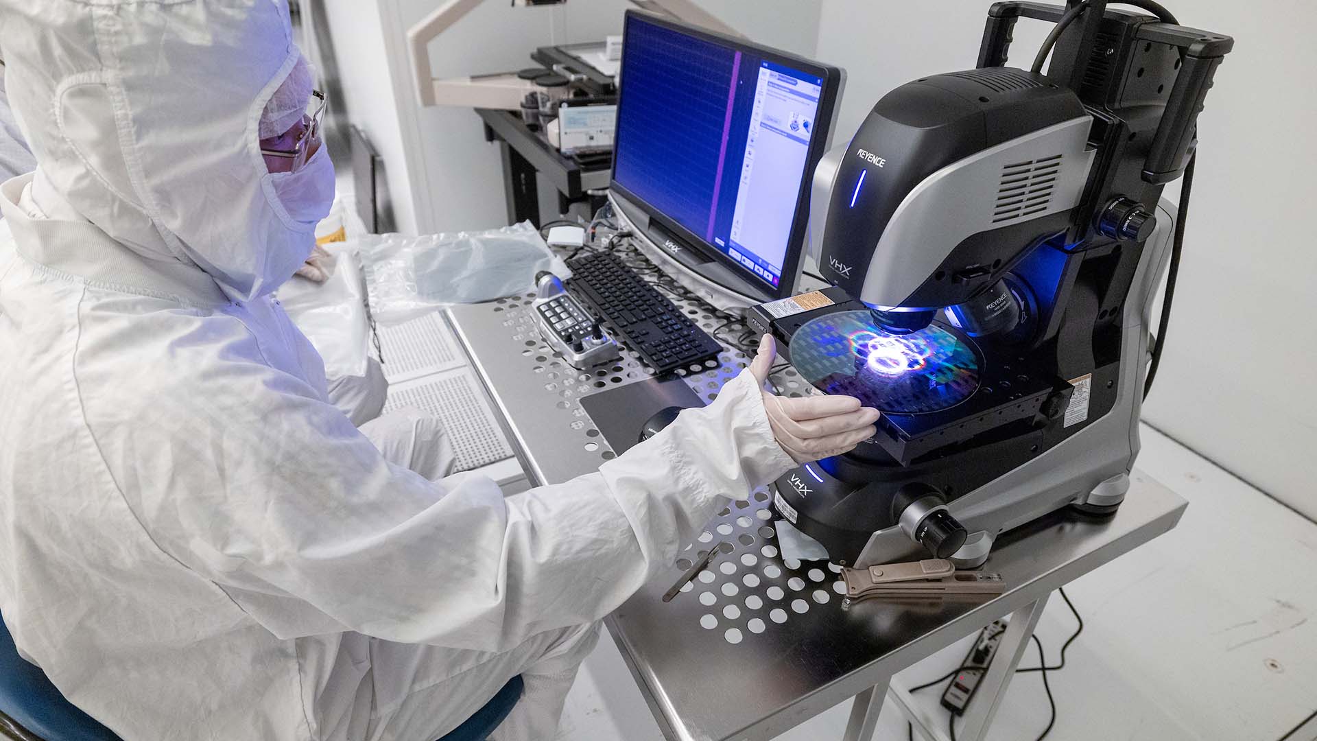
Explore semiconductor packaging at ASU’s cutting-edge labs. Earn $4,000, get housing, and work with industry leaders like Intel.
About the summer research program
Applications for 2026 have closed.
This program is a 6-week immersive National Science Foundation Research Experience for Undergraduates (REU) focused on advanced semiconductor packaging and heterogeneous integration. Work inside ASU’s Nanofab and MacroTechnology Works (MTW) facilities while engaging with industry leaders including Intel and Deca Technologies.
What you receive
- $4,000 Student Stipend
- On-Campus Housing
- Hands-on cleanroom & packaging lab access
- Industry site visits (including Intel)
- Faculty & graduate student mentorship
- Professional networking opportunities
What you’ll learn
- 2.5D and 3D Integration (EMIB, Foveros, Fan-Out)
- Semiconductor Packaging and Assembly
- Reliability and Failure Analysis
- Yield Optimization and Testing
- Multi-Physics Modeling
- Cleanroom Processing and SMT Assembly
Who Should Apply
Undergraduate students in Electrical Engineering, Computer Engineering, Materials Science, Mechanical Engineering, Physics, or related STEM disciplines. Students from ASU, University of Arizona, NAU, and Maricopa Community Colleges are encouraged to apply.
Program Details
Duration: June 1st -July 15th
Location: ASU Tempe Campus
Cohort Size: 24 Students Selected
For more information
Contact Snow Piel with any questions.